-
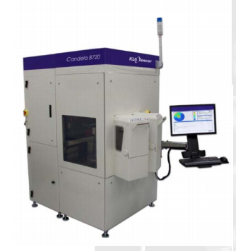
表面颗粒及缺陷检测设备
The Candela Instruments family of Optical Surface Analyzers was first developed for inspection of hard disk substr
-
探针式台阶仪
Bench Top Profilers: • D500 D600 • Designed for simple profiling needs • P-7 P-17 Profilers • Advanced
-
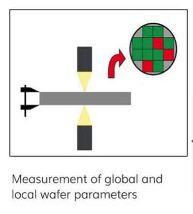
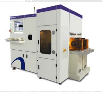
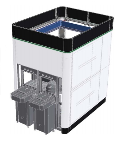
样片厚度及翘曲检测设备
None contact measurement :
1 TTV Bow Warpage Wafer Thickness
2 Surface profile
3 Film thickness
4 Film stress
-
傅立叶变换红外光谱仪
硅中杂质分析---硅中间隙氧和代位碳含量的检测外延层厚度的测定---外延层厚,采用干涉图差减方法---外延层薄,采用倒谱计算方法钝化层分析-
-
光学轮廓仪
-
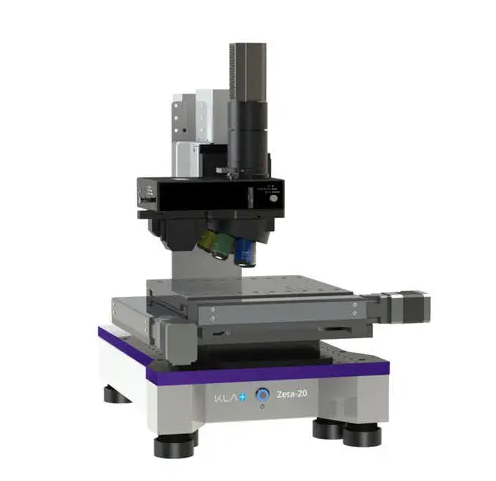
原子力显微镜
Over 33 years experience for AFM tools
• Scan length: 50*50um or 100*100um
• Z scanner: 15um, 30um
• Profiler noise: < 0 02nm
• Stage movement X-Y: 150*150mm or 200*200mm
• Stage movement Z: 25mm
Wafer size: 2” 3” 4” 6” 8?
-
膜厚测试设备
Thin-film thickness of samples up to 450 mm in diameter aremapped quickly and easily with the F50 advanced spectralreflectance system The motorized r-theta stage movesautomatically to selected measurement points and providesthickness measurements as fast as two points per second TheF50 has the same precision high-lifetime stage that performsmillions of measurements in our production systems
-
层厚测量仪
我们具有很好的技术积累并努力达到最高性价比
软件和算法为自主开发,可按客户需求进行定制化改进
设备硬件系统为自主生产以节省成本,最大化优化客户的投入产出比
我们与客户共同努力让机台呈现出最好的性能,并更具您的需求定制小型机或者全自动机台
我们提供及时的技术服务支持
-
套刻及线宽检测设备
MueTec—Overlay and CD measurement
• With Vistec microscope, laser focus, automatic tool
CD (Critical Dimension)
VIS: Down to 0 5 um
UV: Down to 0 3 um
Overlay
Accuracy: 3nm
*IR function